


Applied Materials commits $5 billion to India’s chip ecosystem
The equipment maker’s India expansion reaches beyond fabs to research, precision suppliers and engineering talent. Turning that network into global orders will take years.
Applied Materials’ September 17 announcement sets out a $5 billion investment plan for India through 2035, with research, suppliers and workers central to the plan. The commitment covers research, supplier development and talent, rather than a new chip fabrication plant owned by the US equipment maker.
The plan can still be consequential. Semiconductor manufacturing depends on a dense layer of equipment engineering, process know-how, cleanroom support and qualified suppliers. India has approved multiple manufacturing projects, but Reuters reported that large-scale wafer fabrication had not begun when the commitment was announced. Applied Materials is therefore investing around an industry that is still moving from approvals and construction towards repeatable production.
A September EY–IESA report estimates India’s semiconductor market at nearly $64 billion in 2026 and projects $200 billion by 2035. That would create a much larger customer base, although market demand alone does not guarantee local production.
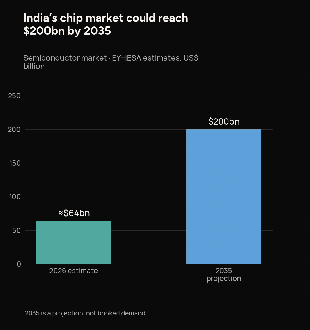
Chart: Technology Index · Data: EY–IESA
Indian suppliers will need to meet semiconductor-grade specifications. Research facilities must solve problems customers will pay to use, while engineering teams need time to develop specialised knowledge.
The money is aimed around the fab
According to Reuters, the investment is intended for research, supply-chain development and workforce expansion. Financial Express reported that the programme includes a proposed 140-acre Advanced Semiconductor Research Park in Bengaluru, cleanroom infrastructure and expansion of the company’s existing research footprint.
That is different from financing wafer capacity directly. Applied Materials sells and supports the complex systems used to deposit, shape and inspect material during chip production. Its India investment can lower the cost of engineering and localisation for customers, but it does not remove the need for foundry operators to commission lines, qualify processes and win orders.
The separation is useful for investors and suppliers. A research park can attract engineering activity before local fabs reach volume. Supplier development can reduce dependence on imported subassemblies. Neither is proof that local vendors have passed the quality, traceability and delivery tests demanded by chipmaking equipment.
Tenfold capacity needs a defined baseline
Applied Materials has said it wants to increase its India supply-chain capacity tenfold and expand its supplier network to more than 100, according to Financial Express. The company has not disclosed a monetary baseline for that tenfold comparison in the material reviewed by Technology Index.
The missing denominator limits what can be inferred. Ten times a small current base may still leave the most specialised components imported. A supplier count can also rise without a similar increase in the value or technical complexity sourced locally. The better milestones will be purchase value, component criticality, qualification rates and the share of suppliers serving global programmes rather than one domestic project.
There is also a sequencing problem. Suppliers will invest in precision manufacturing only when they can see durable demand. Fabs need qualified suppliers before they can operate reliably. Applied Materials can reduce this coordination gap because it sits between tool design, customer processes and the vendor base, but the announcement does not disclose purchase guarantees or supplier-specific capital commitments.
Bengaluru remains the knowledge centre
The plan reinforces Bengaluru’s role in semiconductor engineering. Applied Materials intends to more than double its India research and development workforce by 2035 and deepen university partnerships, Financial Express reported. That is a long runway, and the quality of the work matters more than the eventual headcount.
For India, the valuable outcome would be ownership of harder engineering problems: process integration, materials research, subsystem design, software and field learning from operating fabs. A larger services or support workforce would still create jobs, but it would not carry the same strategic weight.
The research park could help by placing suppliers, customers and researchers near shared cleanroom infrastructure. Its test will be utilisation. Facilities become productive when access rules, intellectual-property terms, equipment availability and project selection are clear. Acreage is an input, not a research result.
The first proof points are commercial
Applied Materials’ commitment arrives as India is offering more than $21 billion in semiconductor incentives and expects domestic chip consumption to rise sharply, Reuters reported. The policy environment provides demand and subsidy signals, but equipment ecosystems are built through repeated production cycles.
Four disclosures would make the $5 billion plan easier to assess: annual spending rather than a 2035 total, the current baseline behind the tenfold supplier target, the number of suppliers qualified for global programmes, and the type of research work moving into customer manufacturing.
The announcement is best read as infrastructure around India’s semiconductor ambition. It can improve the odds that approved fabs acquire local engineering depth and a more resilient service network. It does not prove that those fabs will ramp on time, that local vendors will win high-value work or that research will become commercial process technology.
For prospective suppliers, qualification for Applied Materials’ global programmes would be a more durable prize than a place on a domestic vendor list. Purchase orders and repeat contracts will show how much of the investment reaches them.
One email. Saturday morning.
The week that mattered.
The five stories you needed to read, the data point of the week, and what to watch. From Technology Index editors. No ads, no fluff.